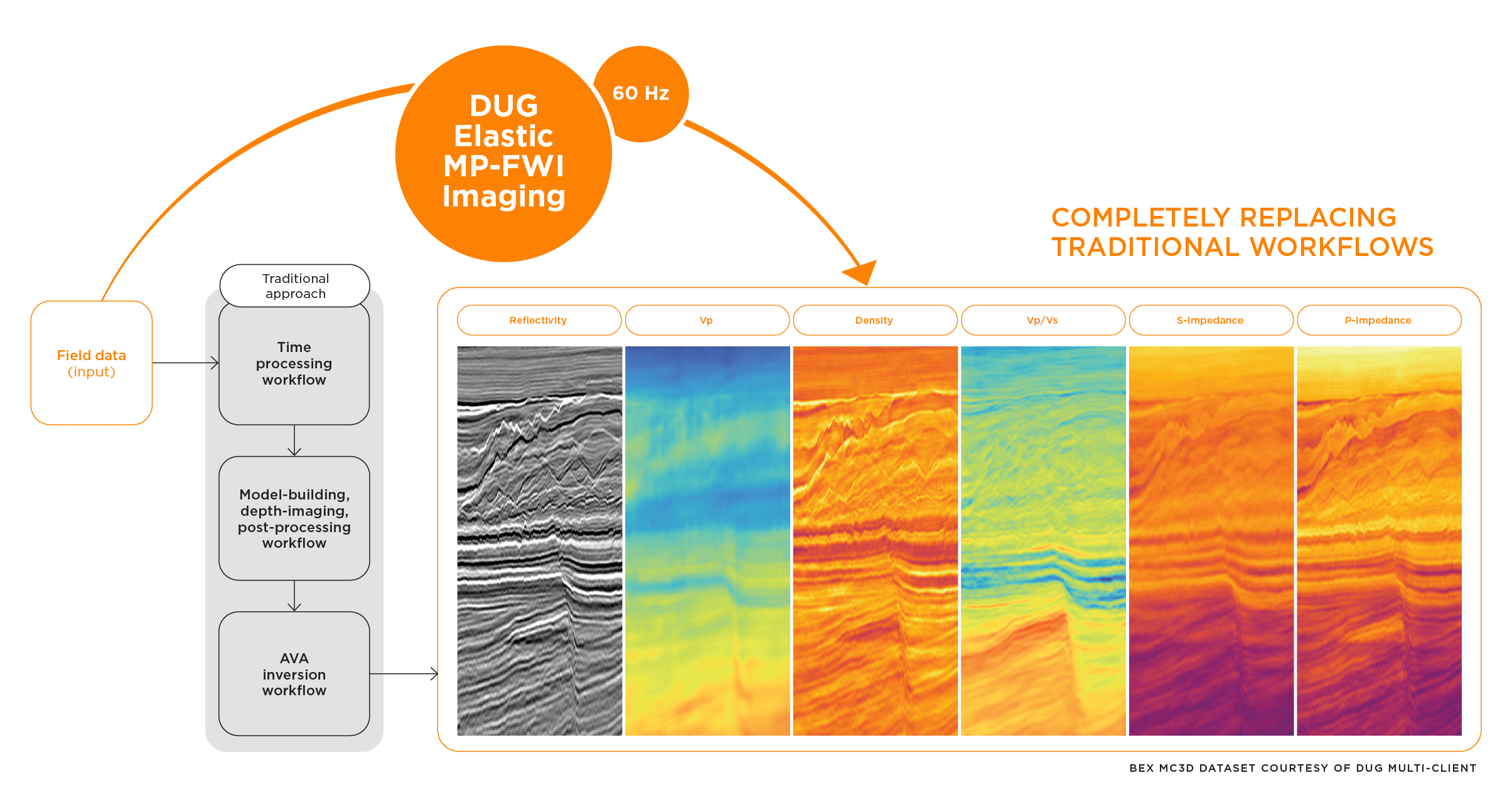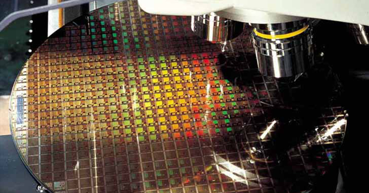
TSMC (Taiwan Semiconductor Manufacturing Company Limited), a company at the forefront of semiconductor manufacture, recently announced a 3 nanometre process, planned for 2022.
This is an incredible milestone. Today, most chips are manufactured using a 7nm or larger process. Reductions in feature size allow more transistors to be packed onto a chip. Chip designers use the increased density to pack more processing cores, memory and storage into the same space. Significantly, with smaller transistors, the energy required for a fixed amount of work decreases.
Phones and laptops using this technology can use less power, potentially extending battery life or providing new features.
In the HPC world, we strive to maximise the density of a data centre. Data centres are rapidly becoming one of the largest global consumers of electricity and reducing power consumption can have a significant impact. Furthermore, this technology will allow existing data centres to meet future demands inside existing space and power envelopes.
Image courtesy of Taiwan Semiconductor Manufacturing Co. Ltd.