Imagine only needing to charge your phone every four days. Imagine smooth-sailing Zoom calls with zero lag. Or a world where we can really trust self-driving cars to avoid collissions.
IBM is the closest to making these dreams a reality with their latest technological breakthrough.
IBM has just unveiled new semiconductor chips with the world’s smallest transistors to date, the tiniest components are smaller than a strand of DNA!
In terms of process node scaling, the new 2 nanometer (nm) chips use nanosheet technology instead of the widely used FinFET technology.
This allows IBM to squeeze 50 billion transistors on a chip the size of a 150 mm2 fingernail.
But wait – what do these numbers even mean?
Packs a bigger punch.
Semiconductors, the foundation of data processing chips at the core of computing, are a critical component in everything from our appliances to mobile phones, transportation systems, infrastructure, and even national defence systems.
Transistors are built from semiconductors. They are the electronic switches that let chips perform logical operations and store data. Transistors are manufactured on silicon wafers, which contain hundreds of individual chips. High-tech cookie sheets, anyone?
The more densely packed the transistors are on a chip, the more calculations it can perform using the same amount of power.
IBM claims a performance increase of 45% or a reduction of power consumption by 75%, compared to the 7 nm node chip.
In practical terms, the new IBM chip is basically smaller, faster, cheaper and more energy efficient – the hardware holy grail for tech companies.
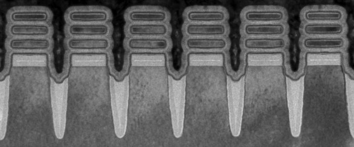
Row of 2 nm nanosheets seen using transmission electron microscopy (TEM). Photo credit: IBM
Raising the bar in chip technology.
How does IBM’s new technology compare to its competitors?
Well it has to be clarified that in the past these dimensions were indeed a direct indicator of the metric for 2D feature size on the chip (such as 90nm, 65nm or 40nm).
But nowadays with the arrival of 3D transistor design (e.g. FinFETs – today’s dominant gate design), the process node name is now an interpretation of the “equivalent 2D transistor design”.
So while IBM’s process node is called “2 nm”, the transistor dimensions do not resemble a traditional expectation of what a 2 nm node might be.
Some features on the chip are in low single digits in actual nanometers, but it’s important to note the disconnect in how process nodes are currently named.
Perhaps a better metric would be the transistor density.
TSMC’s most advanced 5 nm chip, which is used by Apple’s M1 chip computers and A14 Bionic chipset for its iPads, features 171 MTr/mm2
But for IBM’s new chip, 50 billion transistors on 150 mm2 equals a transistor density of 333 million transistors per square millimeter (MTr/mm2).
That’s almost twice the transistor density!
More transistors on a chip will also open up more possibilities for processor designers to integrate different core-level innovations.
It’ll improve capabilities for leading edge workloads such as artificial intelligence (AI) and cloud computing.
It will also pave new pathways for hardware-enforced security and encryption.
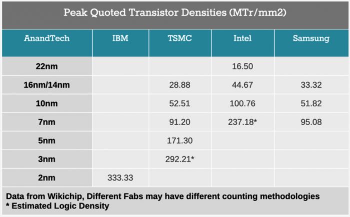
Comparison of transistor densities of current nodes. Photo credit: Dr Ian Cutress/anandtech.com
Tiny chip, huge impact.
Besides drastically improving various technologies, the advent of the 2 nm nodes will also pave the way for greener HPC.
Data centers are energy-intensive enterprises. High-performance computing accounts for an estimated 1 % of worldwide electricity use. This number will only grow with our increasing demands for AI, smart and connected energy systems, autonomous vehicles, and biotechnology.
IBM envisions that the new chips could significantly slash the carbon footprint of data centers. They believe if every data center changed their servers to 2 nm chip processors, enough energy could be saved to power 43 million homes.
This is awesome news for HPC. With the boom in big data processing, supercomputing facilities are striving to adopt new and efficient technologies in the quest of carbon-free computing.
Before we get too excited, IBM’s 2 nm chip is predominantly a proof of concept and it’s still in early development. The processors that’ll build on the 2 nm node are probably at least 2 – 3 years away.
Will this new tech push us closer to the end of Moore’s Law?
We are extremely excited to witness the advancements that IBM’s new chip will certainly bring to the supercomputing realm.
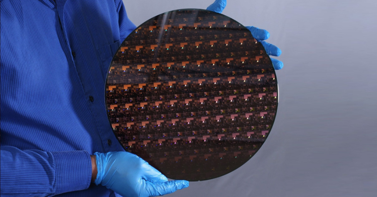
Main picture: A 2 nm wafer fabricated at IBM Research’s Albany facility, containing hundreds of individual chips. Photo credit: IBM