Quantum computing technologies have been progressing by leaps and bounds in recent years. From the establishment of the “99% quantum accuracy club” to the newfound ability to correct quantum errors in real-time and IBM’s grand ambition to develop a 1,121-qubit machine by 2023, many announcements and advancements have left proponents of quantum computing entangled with excitement.
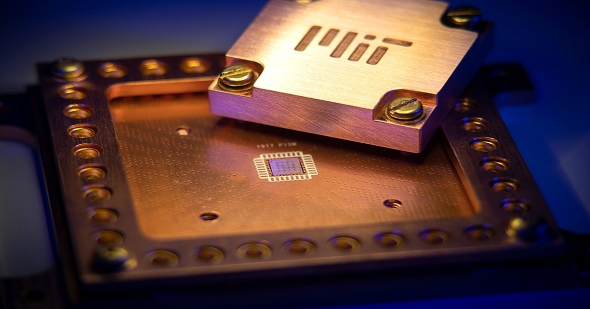
However, many technical hurdles still lie ahead on the quantum brick road—it’s a devilishly complicated technology after all. Of myriad challenges, some crucial ones that stand out are miniaturisation and qubit quality. Like transistors in a conventional computer, superconducting qubits are the building blocks of quantum computers. While transistors have been shrunk close to their physical limits—in the order of nanometres—qubits remain in the millimetre range. Because of their size, quantum devices are currently limited to huge, bulky machines.
Now, researchers at the Massachusetts Institute of Technology (MIT) have forged a better path towards scalability with the development of ultra-thin materials for making qubits.
The quantum quandary.
Published in Nature Materials, the research team, led by Professor William Oliver, managed to formulate superconducting qubits that are not only at least one-hundredth the size of conventional designs but are also less susceptible to error-inducing interference between neighbouring qubits.
Similar to conventional electronic devices, superconducting qubits consist of circuits containing inductors and capacitors. A capacitor, which stores electric field energy, takes the form of a sandwich, where an insulating or dielectric material is wedged between two metal plates.
But unlike typical electronic devices, superconducting quantum circuits only thrive in frosty conditions of less than 0.02 degrees above absolute zero (-273.15 degrees Celsius or -459.6 degrees Fahrenheit). Here’s where issues arise—most common insulators, such as silicon oxides or silicon nitrides, have many defects when operating in this regime, resulting in the loss of quantum coherency.
To circumvent these material shortcomings, most superconducting circuits use what are called “coplanar capacitors”, something like an open sandwich, where there is no top plate and a vacuum sits above the bottom plate to act as the insulating layer—positioned laterally to one another rather than on top of each other. But this arrangement comes with its irksome challenges too—the size of each qubit becomes much larger and there might be undesirable cross-talk between them, diluting quantum information.
Hybrid materials for efficient quantum circuits.
The MIT researchers decided to ditch the open sandwich arrangement and pursue the original idea of a capacitor that is composed of two electric plates with a very clean insulator in between.
Key to this development is a unique material called hexagonal boron nitride (hBN), which can be thinned down to one layer of atoms that is crystalline and defect-free. The advantageous properties of hBN then allow the researchers to stack the atomic layers in desired configurations.
To fabricate the whole capacitor, the MIT researchers meticulously sandwiched hBN between very thin layers of another material called niobium diselenide, which are known for its quantum superconductivity. The resulting sandwich structure renders the capacitor footprint much smaller, while significantly suppressing the cross-talk between neighbouring qubits. This ensures that the performance of the qubits is not sacrificed in return for their number.
Moving forward, the researchers plan to further explore this method to build more qubits on a chip, verifying that their technique eliminates interactions between the qubits. More excitingly, the groundwork the MIT team has laid out will serve as a road map for investigating other hybrid 2D materials to build superconducting circuits that are scalable and defect-free, ushering in the era of practical quantum computing.


