Microchip researchers have once again pushed the limits of Moore’s Law: an observation made by inventor Gordon Moore, that the number of transistors in a dense integrated circuit (IC) doubles about every two years.
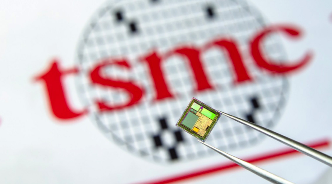
Taiwan Semiconductor Manufacturing Company (TSMC), the world’s largest chip foundry, and its research partners from the National University of Taiwan (NTU) and Massachusetts Institute of Technology (MIT) jointly made a technological breakthrough in the development of 1-nanometer (nm) chips.
Innovating semiconductor materials.
The core of this innovation revolves around using the semi-metal bismuth (Bi), in place of silicon, as the basis for new transistors to resolve one of the biggest problems in miniaturising semiconductor devices.
According to their research published in the journal, Nature, the discovery was first made by the MIT team, with TSMC optimising the deposition process and improved by NTU’s Department of Electrical Engineering and Optometrics.
With bismuth as the transistor’s contact electrode, the contact resistance between the metal electrode and the monolayer semiconductor material can be reduced substantially. An ‘easy deposition process’ was achieved using a helium ion beam (HIB) lithography system.
The flow of electrical current is also increased, allowing the technology to achieve energy efficiency close to the existing physical limits of semiconductor chips.
Pushing the boundaries in semiconductor technology.
Just a few weeks ago, IBM announced the first 2-nm chip that boasts a 45% increase in performance or a 75% slash in power consumption, though commercial production will likely be 2-3 years away.
Present-day technology already has the capability to produce chips down to the 3-nm scale, with production by TSMC slated to start in the second half of 2022.
This 1-nm node breakthrough could potentially break the limits of Moore’s Law. This engineering “rule of thumb” predicts the number of transistors that can be packed onto a microchip will double every couple of years – which roughly equates to a doubling of compute capacity.
When 1-nm nodes become a reality, perhaps it’s time to express photolithographic chips in angstroms (Å), and retire the current unit of length, nanometers (1 Å = 0.1 nm) – though that will only be sufficient for a decade at the current pace of advancement.
Still in its technological infancy.
While this is absolutely great news, TSMC has also clarified that their newly developed process may not be used in high volume manufacturing in the foreseeable future.
Their 1-nm node is currently in its path-finding and exploratory R&D stage, and they are experimenting with various other options. Even the usage of their new material bismuth is not guaranteed.
But above all, one thing is for sure – this is a stellar demonstration of human innovation and bodes well for the computing industry’s desire for more compute with less energy consumption.
As evidenced by TSMC’s progress, microchip scientists are already breaking new grounds in developing nodes close to the physical limits.
Expect your electronic devices to be packed with chips beyond the 1-nm node in the not-too-distant future.


